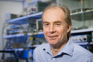
Compound Semiconductors are tiny electronic chips that drive tomorrow’s technologies. Faster and more versatile than silicon, they are found in a range of leading-edge products, from mobile phones to electric vehicles. Along the M4 corridor, businesses and academic institutions have been working on CS for decades – from pure academic research through to device design and wafer manufacture. Now, a major UKRI investment project – led by Cardiff University – is putting the infrastructure in place to bring the partners together as CSconnected – the world’s first CS cluster. Here, Professor Peter Smowton, Director of the Institute for Compound Semiconductors (ICS), explains how ICS will help shape CSconnected’s future in South Wales.
 “We were all doing different things, working on CS technologies but not really working together, for many years. Then, about five years ago, we realised we’d be more effective together. Since establishing ICS in 2015, we’ve helped to build the framework to support the cluster.
 First, we were a founding member of CSconnected when the original cluster vision was formed. Then, along with world leading Cardiff-based wafer manufacturer, IQE we established the Compound Semiconductor Centre – a joint for-profit venture.. In turn, this helped to leverage £50m from UK Government for the CS Applications Catapult. We recruited experienced and specialist CS process engineers from both industrial and research backgrounds and have gone on to develop new technical processes – like fabricating tiny VCSEL laser pulsing devices (commonly used in mobile phones for face recognition). And we have branched out to work with more than a dozen different local organisations via collaborative projects.
Not only that. Our vision of being stronger together as a cluster helped us attract funding to build a new 1500m2 cleanroom – currently taking shape on the University’s new Innovation Campus (CIC) on Maindy Road in Cardiff. The ERDF-funded ICS is now focusing on the technologies to be installed, ensuring we deliver the flexible, industry-standard CS fabrication facility required by the CSconnected cluster, and all users across the UK.
We will house a range of equipment selected to deliver the widest range of process steps possible and staffed by experienced Process Engineers capable of working with our users to ensure they get the most from the facility.
In essence, this is our role in the cluster: providing a flexible and reconfigurable fabrication facility where users can develop and refine complex CS process flows for wafers up to 8” in diameter, all under one roof.
This was simply not possible before. Soon it will be right on the doorstep of the CSconnected cluster and at the right time, because this flexibility is required now to rapidly develop the widest range of CS devices for application in exciting future technologies such as ‘LiFi.’
Society is running out of available frequencies in the radio wave spectrum for WiFi due to an increase year on year of wireless data usage. By transmitting data using pulsed light sources (LEDs, lasers) instead – ‘LiFi’ – not only opens up the light spectrum to ease this shortage but can transmit data much faster – at the speed of light.
Miniature Atomic clocks, too, need CS technology. These precise timing devices are vital in modern life. Underpinning the Global Navigation Satellite Systems (GNSS), they enable safe transport links, mobile communications, data networks and electronic transactions. And at the heart of every miniature atomic clock is a VCSEL – manufactured from compound semiconductor material.
Solar Photovoltaic (PV) Cells are a vital technology as we transition to a low carbon society. The very best conventional silicon PV cells are only about 30% efficient. By stacking multiple layers of compound semiconductors with different band gaps, known as a tandem or multi–junction solar cells, this efficiency could be increased enormously, theoretically up to 86%.
The Institute’s skilled process engineers are currently further developing a range of, currently, full 6” processes to act as generic baseline platform for CS devices with interesting and exciting properties – from GaAs, VCSELs and GaN LEDs to GaN MMICs. This is critical for improving processing capabilities and industrial engagement.
By establishing these processes, we demonstrate our capabilities to our users, who can then either purchase these standard devices from us or work collaboratively with us to develop and fabricate devices to their own specification.
The ICS also seeks to develop integrated CS and silicon manufacturing in the longer term, reducing the cost of CS device development, manufacturing and therefore market price by leveraging well-established low-cost silicon manufacturing methods.
Naturally, we were delighted that this month, UKRI saw fit to support the £44m project, through its Strength in Places Fund to establish CSconnected as a stand-alone entity, working closely with 12 partners across the South Wales cluster.
We look forward to the next five years. Post-COVID-19, the developments set in motion by the ICS will provide a significant boost to the field, ensuring that the UK and south Wales are firmly on the map as world leaders in CS technology.
